Advanced Materials, Electronics & Communications
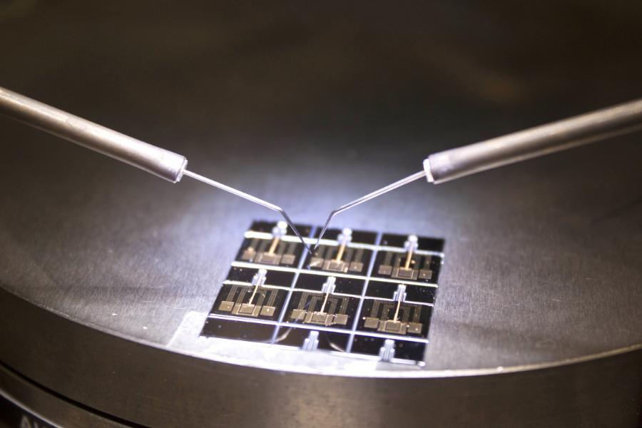
In this challenge, our members carry out research which aims to exploit the electronic, physical, chemical and biological properties of materials with dimensions from the nanoscale upwards. This high impact work has applications in sensors, actuators and next generation communications. It is supported by extensive cleanroom, electromagnetic testing and other laboratory facilities within the Department.
Advanced Materials, Electronics & Communications aligns with goal 12 of the United Nation's Sustainable Development Goals: Responsible Consumption and Production - Ensure sustainable consumption and production patterns.

Areas of Research Interest
Examples are given below of the research that is currently being carried out by AMEC members.
Communications
- 5G & higher frequency bands for wireless communication, high speed trains and radar
- Sustainable cloud radio access networks and machine learning in wireless communications
- Mm-wave and THz device and antennas
- Wireless channel characterisation
- Intelligent reflecting surface aided wireless communication systems
These activities are supported by facilities which include an anechoic chamber, channel sounders, a THz vector network analyser and a time domain spectroscopy system.
Energy Materials and Systems
- Degradation effects on organic solar cells
- Structural electrolytes for multifunctional energy storage devices
- Rectenna based energy harvesting
- Flexible thermoelectric devices
- Energy management in aerospace under fault conditions
Materials processing can be carried out in the Challenge’s cleanroom facilities which, for example, include nitrogen gloveboxes for the handling of materials that are sensitive to oxygen.
Health and Wellbeing
- Advanced materials and modelling for healthy living
Nanotechnology
- Integration of nanomaterials in device fabrication
- Charge transport dynamics in low dimensional and nanostructured semiconductors and their application as sensors, memory devices and logic
- Degradation effects on evolutionary processors
The nanotechnology research is supported by our cleanroom fabrication facilities and also associated metrology and test equipment.
Sensors
- Wearable pressure sensors based on 2D and 3D nanophotonic metamaterials
- Strain gauge development for Internet of Things applications
- Metamaterials for biosensing
- Harnessing quantum defects for novel metrology
This research relies on our expertise in cleanroom-based photolithography and thin film deposition & etching.


/prod01/prodbucket01/media/durham-university/departments-/engineering/74202-5112X1676.jpg)